Printed Circuit Boards (PCBs) serve as the essential structural and electrical infrastructure of modern electronic systems. Every device that processes information, transmits signals, or manages power relies on a PCB to function reliably. From smartphones and automotive control units to aerospace navigation systems and industrial robotics, PCBs provide the controlled environment where electrical components operate together as a cohesive system.
This comprehensive guide explains PCB technology from a technical and educational standpoint. It explores how boards are engineered, how signals behave across layers, how manufacturing affects performance, and how global production ecosystems influence quality and scalability. The objective is to provide a structured, accurate overview aligned with industry standards and engineering best practices.
What Is a Printed Circuit Board?
A Printed Circuit Board is an insulating platform layered with conductive copper traces that mechanically support and electrically connect electronic components. Instead of using manual wiring between components, PCBs allow designers to create organized, repeatable, and compact circuits.
At a fundamental level, a PCB integrates:
- Electrical routing pathways
- Structural reinforcement
- Controlled power distribution
- Thermal management channels
This combination enables devices to operate safely and efficiently within defined performance parameters.
The Engineering Principles Behind PCB Performance
Understanding PCB technology requires understanding the physics governing it.
Electrical Conductivity and Trace Design
Copper traces conduct electrical current across the board. Their width, thickness, and length affect resistance and heat generation. For high-current applications, thicker copper is used to prevent excessive temperature rise.
In high-speed circuits, trace design also determines signal timing accuracy. Signal distortion may occur if impedance is not properly controlled.
Dielectric Materials and Signal Propagation
The substrate material—often FR-4 fiberglass epoxy—acts as a dielectric medium between conductive layers. Its dielectric constant influences signal velocity.
For high-frequency communication systems, advanced low-loss materials are selected to minimize signal attenuation and preserve integrity.
Thermal Management Engineering
Electronic components generate heat, and thermal buildup reduces reliability. PCB layouts incorporate:
- Copper pours for heat spreading
- Thermal vias beneath power devices
- Heat sinks and airflow channels
Managing heat effectively extends component lifespan and enhances system stability.
PCB Layer Structure and Architecture
Modern PCBs are multilayer structures carefully engineered to separate signal types and improve electrical stability.
Signal Layers
Carry data and communication pathways between components.
Power Planes
Distribute voltage evenly and reduce electrical noise.
Ground Planes
Provide a stable electrical reference and electromagnetic shielding.
Vias and Microvias
Enable vertical interconnection between layers. High-density boards use microvias to support compact device designs.
Layer stacking order plays a critical role in reducing electromagnetic interference (EMI) and improving signal integrity.
PCB Design Workflow: From Concept to Fabrication Files
Professional PCB development follows a systematic process.
1. Schematic Capture
Engineers define electrical relationships and component functions.
2. Layout Planning
Components are placed to minimize signal path length and optimize thermal flow.
3. Routing and Constraint Management
Trace widths, spacing, and impedance are calculated based on current load and frequency requirements.
4. Design Rule Verification
Software tools check for spacing violations, clearance errors, and manufacturability concerns.
Design decisions must account for real-world fabrication capabilities and assembly tolerances.
PCB Fabrication: Industrial Manufacturing Explained
Fabrication transforms digital layout files into physical boards.
Imaging and Copper Etching
Photosensitive film defines circuit patterns. Excess copper is chemically removed.
Drilling and Copper Plating
Precision drills create vias and mounting holes. Copper plating connects inner layers electrically.
Lamination
Multiple layers are bonded under high heat and pressure to form a single rigid structure.
Surface Finishing
Surface treatments such as ENIG (Electroless Nickel Immersion Gold) enhance solderability and prevent oxidation.
Comprehensive electrical testing ensures no open circuits or short circuits exist before assembly.
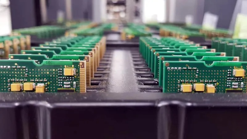
PCB Assembly and Global Production Ecosystems
After fabrication, boards proceed to assembly, where components are mounted and soldered.
Surface Mount Technology (SMT)
SMT allows automated placement of compact components, enabling high-density production.
Through-Hole Assembly
Used for high-strength connectors and power components requiring mechanical durability.
Functional Testing
Completed boards undergo operational verification to confirm performance compliance.
Global manufacturing ecosystems play a significant role in PCB production scalability. Countries with strong electronics infrastructure provide integrated fabrication and assembly services. Many companies evaluate partnerships related to pcb assembly in china to balance cost efficiency, quality assurance, and production capacity.
For broader insight into international manufacturing frameworks and production capabilities, professionals often research resources related to pcb assembly in china when evaluating large-scale deployment strategies.
Reliability, Quality Control, and Industry Standards
Reliability is a primary concern in PCB engineering, particularly in safety-critical applications.
Common Failure Modes
- Solder joint fatigue from thermal cycling
- Via cracking due to expansion mismatch
- Delamination between internal layers
- Corrosion from moisture exposure
Quality Certifications
Reputable manufacturers comply with:
- IPC standards (e.g., IPC-A-600, IPC-6012)
- ISO 9001 quality systems
- RoHS environmental compliance
Inspection technologies include:
- Automated Optical Inspection (AOI)
- X-ray analysis
- Flying probe electrical testing
These processes ensure long-term performance stability.
Industry Applications of PCBs
PCBs power innovation across numerous sectors.
Consumer Electronics
High-density multilayer boards support compact smartphones and laptops.
Automotive Electronics
Control systems must withstand vibration, heat, and electromagnetic noise.
Telecommunications Infrastructure
Signal integrity and impedance control are critical for high-speed data transmission.
Aerospace and Defense
Boards operate in extreme temperature and mechanical stress conditions.
Medical Devices
Reliability and compliance are essential for patient safety.
Each industry imposes unique design and testing requirements.
Emerging Trends in PCB Engineering
PCB technology continues evolving alongside digital transformation.
High-Density Interconnect (HDI)
Microvias and fine traces enable smaller, faster devices.
Flexible and Rigid-Flex Boards
Support innovative product form factors.
Embedded Components
Passive devices integrated within layers reduce size and improve reliability.
Smart Manufacturing
Artificial intelligence improves defect detection and production yield.
Sustainability and Environmental Responsibility
Environmental regulations have reshaped PCB manufacturing practices.
Lead-Free Soldering
RoHS compliance restricts hazardous materials.
Chemical Waste Management
Etching and plating processes require strict environmental oversight.
Lifecycle Optimization
Durable board design reduces electronic waste.
Sustainability is now integrated into engineering decision-making.
Conclusion
Printed Circuit Boards represent a critical intersection of electrical engineering, materials science, and industrial manufacturing. They transform circuit diagrams into reliable physical systems capable of powering modern technology.
Understanding PCB design principles, fabrication processes, assembly practices, reliability factors, and global production ecosystems allows engineers and industry professionals to make informed decisions that improve product quality and performance.
As electronic devices become more complex and performance-driven, PCB innovation will remain central to technological advancement across industries worldwide.